Just over three years ago, the U.S. approved $52 billion in funding for the CHIPS for America Act and passed this into law the following year through the CHIPS and Science Act of 2022. The idea was to encourage firms to support local manufacturing supply chains, and train future talent for the industry.
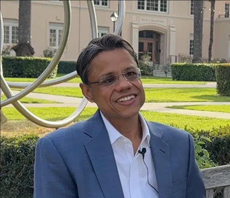
Earlier this month, we sat down with Sanjay Kumar, a former senior director at the U.S. CHIPS Program Office (Department of Commerce), where he led investment evaluations and negotiations for large-scale semiconductor manufacturing, packaging and supply chain projects, contributing to nearly $30 billion in capital expenditures.
We met in Santa Clara, Calif., to talk about the CHIPS Act award process, as well as the successes and misconceptions around the CHIPS Act awards. Given that Kumar was part of a team that saw many proposals, we also discussed some of the big trends, what a CHIPS Act 2.0 might look like, the strategic importance of multiple suppliers, the need for downstream funding in many parts of the supply chain and more. We even touched on Intel’s key role in this U.S. ecosystem.
Watch the video.
CHIPS for America awards in December 2024
A quick look at the CHIPS for America website shows frequent awards being handed out. Looking just at announcements in December at the time of writing this story, the U.S. Department of Commerce issued a number of awards, including $406 million to subsidiaries of GlobalWafers America to convert a portion of its existing silicon epitaxy wafer manufacturing facility in Sherman, Texas, to silicon carbide epitaxy wafer manufacturing.
In its announcement, the government said these CHIPS investments will support projects with total capital expenditures of approximately $4 billion across Texas and Missouri, and directly support the construction of wafer manufacturing facilities in these states; it is expected to create approximately 1,700 construction jobs and 880 manufacturing jobs across both states.
The facility in Texas will be the first advanced, high-volume 300-mm silicon wafer facility in the U.S. Silicon wafers from this facility will be used in the manufacturing of advanced leading-edge and memory devices. Another facility in Missouri (MEMC, a subsidiary of GlobalWafers) will serve as a key domestic production site for 300-mm silicon-on-insulator (SOI) wafers. SOI wafers from this facility will be a key input for devices used across the defense and aerospace sectors.
In other December announcements:
- Bosch is set to receive $225 million towards its planned investment of $1.9 billion to transform its Roseville, Calif., facility to produce silicon carbide power semiconductors.
- Micron is receiving about $6.2 billion for its long-term vision to expand DRAM production in Idaho and New York, plus $275 million for expansion and modernization of a facility in Manassas, Va., and on-shore Micron’s 1-alpha technology.
- Coherent is getting up to $33 million to support modernization and expansion of a state-of-the-art manufacturing cleanroom in its existing 700,000 square-foot facility in Sherman, Texas, to establish the world’s first 150-mm indium phosphide (InP) manufacturing line by adding advanced wafer fabrication equipment to produce InP devices at scale.
- SkyWater Technology will get up to $16 million to support modernization of its existing facility in Bloomington, Minn., to improve the quality of production and wafer services by replacing equipment, upgrading the facility’s cleanroom and IT systems, and increase overall production capacity of 90-nm and 130-nm wafers by approximately 30%. The company is a Department of Defense Trusted Foundry. As a result of proposed CHIPS funding, the company would be able to improve productivity and enhance operational sustainability to support Department of Defense missions, as well as grow its commercial business. Skywater’s short and long-term workforce development goals will also get $19 million in dedicated funding from the CHIPS program.
- X-Fab is to receive investment of up to $50 million to support the expansion and modernization of its SiC foundry facility.
- Absolics is to receive an award of up to $75 million to support the construction of a 120,000 square-foot facility in Covington, Ga., and the development of substrates technology for use in semiconductor advanced packaging. Currently, the advanced packaging substrates market is concentrated in Asia, and because of this investment, U.S.-based companies will have an expanded domestic supply of glass substrates for advanced packaging. The investment is expected to support approximately 1,200 construction, manufacturing and R&D jobs.
- Entegris will get up to $77 million to onshore critical semiconductor supply chain and manufacturing equipment materials for leading-edge chip production and support Entegris’ construction of its state-of-the-art manufacturing center in Colorado Springs, Colo. The manufacturing center, which is targeted to begin initial commercial operations in 2025, will initially support production of liquid filtration products, as well as front-opening-unified pods (FOUPs). FOUPs are highly specialized containers that secure semiconductor wafers while they are handled and transported during the manufacturing process.
12/24/2024 | Elektrik - Elektronik Mühendisliği
All information, documents, photos, videos, images, texts, etc. on our web pages cannot be used without permission and without citing the source. Otherwise: Legal and criminal action will be taken within the scope of Law No. 5846. All rights of Şırnak University are reserved.