Recognizing that microLED data links depend on tightly coupled technology bricks, CEA-Leti is launching a multilateral partnership to co-develop scalable optical interconnects for future AI systems.
As AI systems scale toward ever-denser GPU clusters and memory-heavy architectures, interconnects are emerging as a primary bottleneck. Compute performance continues to grow exponentially, but the links between processors, accelerators, and memory are struggling to keep pace—both in power efficiency and reliability.
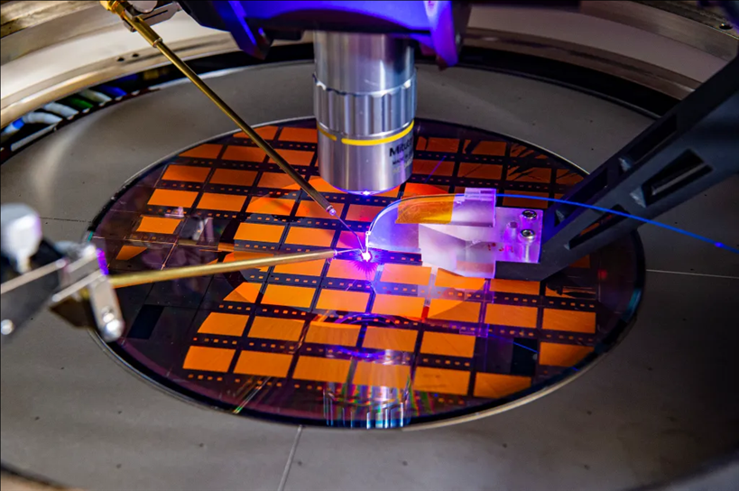
Against that backdrop, CEA-Leti is launching a new three-year multilateral R&D program aimed at accelerating microLED-based optical data links for short- to mid-range, ultra-high-bandwidth communications.

The program is set to begin in early 2026, bringing together a wide cross-section of the microelectronics and photonics value chain, from microLED emitters and fiber suppliers to chipmakers, system integrators, and hyperscalers. The goal is to develop scalable, manufacturable microLED interconnect technologies that can deliver orders-of-magnitude improvements in energy efficiency and bandwidth density compared with today’s copper and laser-based solutions.
Why microLED, and why now?
The motivation is straightforward. Copper links remain power-efficient and reliable, but their reach collapses as data rates rise, making them impractical beyond very short distances. Laser-based optical links offer longer reach, but at the cost of high power consumption, complex packaging, and declining reliability at scale. Interconnect performance is no longer keeping up with compute growth—and that creates a widening gap that threatens next-generation AI systems.
MicroLEDs promise a different trade-off. Originally developed for display technologies, microLEDs are orders of magnitude smaller than conventional LEDs and can be directly modulated at several gigabits per second using simple on-off signaling. Because they operate at much lower power than lasers and can be fabricated in dense arrays, microLEDs open the door to massively parallel optical links—many slow channels rather than a few extremely fast ones.

This “wide-and-slow” architecture is at the heart of MOSAIC, a microLED-based optical interconnect concept recently detailed by Microsoft Research. In that work, Microsoft demonstrated a prototype optical link using hundreds of parallel microLED channels combined with multicore imaging fibers, achieving up to 68% lower power consumption than today’s optical links, ten times the reach of copper, and significantly higher reliability.
CEA-Leti’s program builds directly on this architectural insight, and aims to translate it from research prototypes into scalable, industrially relevant technologies. Unlike many past R&D efforts, which relied on bilateral collaborations between a research institute and a single industrial partner, CEA-Leti deliberately chose a multilateral program structure for microLED data links.
Because there are so many technical aspects that need improvement at the same time, the best way to make progress is to put players from different parts of the ecosystem in one room, according to Vygintas Jankus, partnership manager for microLED technologies at CEA-Leti. “A change in one brick impacts another brick’s parameters,” Jankus told EE Times in an exclusive interview. “If different partners go in different directions without coordination, the bricks simply won’t fit together.”
Those “bricks” span a broad value chain: microLED emitters, CMOS driver and receiver electronics, multicore fibers, optical coupling and packaging technologies, and system-level integration. According to Jankus, system integrators and hyperscalers are also critical participants because they help define realistic specifications from day one.
“Emitters, fibers, packaging, system integrators, design—all of those are important,” he said. “Because one change impacts the others, everything needs to be aligned.”
Accelerating maturity, not just sharing know-how
While partners are expected to bring existing expertise, the program aims explicitly to accelerate the maturity of weaker links in the supply chain. CEA-Leti plans to develop shared test vehicles and joint demonstrators with scalable performance, allowing partners to validate their own technologies against a common roadmap.
“This program is designed to help some segments of the supply chain mature faster than they otherwise would,” Jankus explained. “Fiber suppliers may not have LEDs in-house, LED suppliers may not control packaging or optics—but through the program, they get that information early and can adapt their designs for scalability and manufacturability.”
Partners will receive regular technical updates, access to demonstrators, and licenses to CEA-Leti IP developed during the program. Each company retains ownership of its background IP, while any jointly invented foreground IP will be handled under bilateral agreements.
CEA-Leti has defined aggressive but staged technical targets. Within the first one to two years, the institute aims to demonstrate sub-1 picojoule-per-bit energy efficiency using hybrid-bonded microLEDs integrated with custom ASICs, all fabricated using standard microelectronics processes. A subsequent milestone targets 1.3 terabits per second per millimeter of bandwidth density using industry-standard electrical interfaces, such as UCIe.
By the end of the program, the ambition is expected to rise to 10.5 terabits per second per millimeter at below 0.5 picojoule per bit, figures that would significantly outperform today’s optical interconnects in both power efficiency and density. The roadmap is not rigid, however. “We are very open to discussing optics and packaging elements,” Jankus said. “We’ll start with our proposal, but we’re flexible based on partner input.”
Despite the disruptive potential of microLED interconnects, CEA-Leti does not position the technology as a wholesale replacement for silicon photonics or laser-based optics. Instead, the institute sees a segmented future.
“Every technology has its own place,” Jankus said. “MicroLED-based interconnects make sense for point-to-point links (GPU-to-GPU, GPU-to-memory) for middle-range distances. Silicon photonics is better suited for longer distances and switch-level interconnects.”
The program is also deliberately forward-looking. Rather than targeting near-term pluggable optics, it aims to influence post-2028 architectures where optical links move closer to the compute die itself. “We’re aiming to integrate optical links very near GPUs and memory,” Jankus said. “That implies some time. Real deployment is more in the 2030 timeframe.”
From Jankus’discussions with prospective partners, motivations vary. Some companies see microLED interconnects as a way to avoid hitting a hard “interconnect wall” as AI systems scale. Others are drawn by reliability—microLEDs are inherently more temperature-tolerant than lasers—or by the promise of lower power consumption without exotic manufacturing steps.
Crucially, the program is designed to minimize entry risk. CEA-Leti emphasizes standard foundry-compatible processes and avoids materials that would require greenfield investments. “You don’t need to build a new foundry,” Jankus said. “You can use existing capacities.”
If successful, the multilateral program could do more than validate a new interconnect technology. It could help align an emerging ecosystem around microLED data links—before fragmentation sets in—and provide a credible alternative path for scaling AI infrastructure beyond the limits of copper and conventional optics.
Pat Brans is a contributing writer for EE Times and EE Times Europe. After a 22-year career in high tech, Brans embarked on a new mission as a freelance science and technology journalist. From his home in Grenoble, France, he maintains an extensive network that ranges from highly skilled scientists and technologists to C-level executives around the world. In the 15 years he has been writing professionally, Brans has interviewed over 1000 people and written over 1000 articles. Brans has also taught classes at both graduate and undergraduate levels at Grenoble École de Management and has authored two books: "Master the Moment: Fifty CEOs Teach You the Secrets of Time Management" and "Mobilize Your Enterprise: Achieving Competitive Advantage through Wireless Technology."
1/13/2026 | Elektrik - Elektronik Mühendisliği
All information, documents, photos, videos, images, texts, etc. on our web pages cannot be used without permission and without citing the source. Otherwise: Legal and criminal action will be taken within the scope of Law No. 5846. All rights of Şırnak University are reserved.