Canada’s photonics sector is on the cusp of a renaissance as the technology steps up as a key enabler for AI data centers and quantum computing.
Much like its quantum computing sector, which has a strong foundation to become competitive at a global level, Canada’s photonics foundation is solid, while also being at risk of losing ground without the right investments.
Canada’s history in photonics dates back to the Nortel era—the long defunct Canadian telecom giant provided the majority of photonics devices to the world, and the country is now home to hundreds of photonics companies designing and developing photonic products even though the integrated silicon photonics components are typically built elsewhere.
Lower barrier to entry
Like compound semiconductors, photonic device fabrication is simpler than microelectronics fabricated using CMOS process—sometimes they need only a single lithography step for passive devices, which enables faster prototyping. “Microelectronic CMOs type stuff is vastly more complicated, and your contamination and cleanliness requirements are much more strict,” Aaron Hryciw, fabrication group manager at the University of Alberta nanoFAB Centre in Edmonton, told EE Times in an interview.
This means obtaining capital equipment is less of a barrier to scaling up Canada’s photonics capabilities. “The resolution requirements aren’t so hard,” he said. “You can make good state-of-the-art devices with two micron feature sizes.”
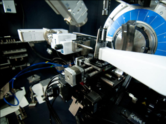
The nanoFAB has built up a significant manufacturing and characterization footprint over the past 25 years catering to a large contingent of small- and medium-sized businesses interested in building their specific type of semiconductor devices, nanoFAB director Eric Flaim told EE Times in an interview. The facility focuses on supporting proof-of-concept prototyping and low-volume manufacturing.

It is fairly technology agnostic, he added, which means photonics is a part of broader mix of research that also includes compound semiconductors and MEMS, among others. “Our role is purely to support the academic researchers who are typically doing their PhD and master’s level work and supporting the north of 50 companies a year that access our capabilities in order to develop and build their actual products,” Flaim said.
He added that there has been a noticeable expansion in photonics related research over the last decade, especially around sensing technologies applicable to Alberta’s natural resource-based industries, whereas photonics activities in a region like Ottawa is more focused on communications.
Flaim said Canada’s Photonic Fabrication Centre (CPFC) in Ottawa is an excellent example of Canada’s photonic fabrication capabilities, but they cannot do everything for everyone. “They have a particular niche that they’re catering towards.”

The Centre de Collaboration MiQro Innovation (C2MI) in Bromont, Quebec, is another example of niche manufacturing capabilities catering to specific industry partners, he said.
The nanoFAB is focused on continuing to increase its manufacturing capability footprint with the help of government funding so that more can be done at home, Flaim said, with a specific focus on dual-use and defense technologies that would include standard semiconductor devices, as well as photonics capabilities.
Going big but staying home
At Accelerated, Canada’s Semiconductor Symposium, Velko Tzolov, CPFC’s director general, said the biggest question facing Canada’s photonic sector is how it will scale up, which is why there is huge incentive for the facility to become a commercial entity as soon as possible so it can help clients scale at the pace they want. “We help them to scale up rather than moving their manufacturing offshore, which we don’t want.”
He said that over the years, CPFC has become part of a global supply chain serving multi-national, billion dollar companies, albeit not by design. “Our Canadian companies got acquired by a bigger company.”
Tzolov said the commercialization of the CPFC could set the stage for expansion of Canada’s fabrication capabilities over the longer term, if not in his lifetime. “Nobody has a crystal ball, but I think it’s coming. That’s exciting.”
Scaling up photonics capabilities is a realistic, and affordable, endeavor, according to Gord Harling, CEO of CMC Microsystems.
Harling told EE Times a production facility for silicon photonics would cost less than CDN$1billion (U.S. $317 million) and could generate the same amount in annual revenue. Such an investment would align with previous investments in photonic packaging made by IBM Microelectronics in Quebec, Harling added, and it could take advantage of the laser light sources produced at the CPFC.
A photonics production facility would also be the natural next step for companies building prototypes at other facilities, such as at 3IT in Sherbrooke, Quebec, the NanoFAB and C2MI, Quebec—volume production would stay onshore rather than going to Europe or Asia.
Photonics and compound semiconductor technologies are also intertwined, and both are target areas for the FABrIC funding program managed by CMC. “There are a lot of new applications that are coming out of silicon photonics, and the fabrication processes are ramping up and becoming more complex. But it’s a great place for us to be because it really is much more about brain power that it is about massive capital investment.”
Quantum computing adds incentive
While AI data centers are a big driver for optical technologies, photonics is also getting more attention because it is an enabler of quantum computing, including the modality being pursued by Photonic Inc. in Vancouver.
“To achieve the ultimate version of quantum, it needs to be a networked version of quantum,” Stephanie Simmons, Photonic’s co-founder and quantum officer, said in an interview with EE Times.
A networked approach to quantum computing allows for both easier manufacturing and modularity, as well as horizontal scaling, she said. Early efforts in quantum computing looked to achieve scale by putting more and more resources into a single box. “My instinct was that we’re going to have to get these boxes working together.”
Simmons said connecting these boxes together across network requires photons. “The photons are the glue and the thing that determines the performance of any scaled quantum system, be it networks or computing,” she said. “The hardest part of quantum is the networking of these quantum systems together.”
She said photonic-based approaches have greatly moved forward in the last two decades. “A lot of the early ideas are now becoming products that are rugged and data center compatible.”
Underinvestment threatens future
Wei Shei, Canada Research Chair in Silicon Photonics based at the University of Laval, said the combination of research and training is critical for advancing photonics to address significant future challenges over the longer term in the semiconductor industry. Research concepts the university published a decade ago are now the basis of technology recently announced by Nvidia, he said. “You never thought this technology would have been in the most advanced, compute systems, but that’s very encouraging.”
Training is also critical, and Canada has a strong track record, Shei said. “We definitely have one of the strongest training systems in the world.”
However, many students end of up leaving for the U.S. for higher salaries, he said, while a dearth of investment in photonics means Canada no longer has the cutting edge tools it once had. “We’re not cutting it anymore.”
Shei said despite facilities like the CPFC, not all researchers can afford access to the most advanced semiconductor and photonics processes. “We could be doing better to keep our leadership.”
Shei added that the goal with any future investments is to establish a stronger ecosystem to address the opportunities for photonics and optical technologies needed for AI and quantum computing.
The latter is still nascent, Shei said, but the consensus is that AI is exploding and with that there is a need for better interconnects to connect powerful GPUs. “Optics will play an essential role.”
He said quantum computing is sexier, but photonics for optical communications is fundamental. “Without that, there’s nothing. Photonics is the backbone of AI, especially in the next decade.”
Gary Hilson is a freelance writer and editor who has written thousands of words for print and pixel publications across North America. His areas of interest include software, enterprise and networking technology, research and education, sustainable transportation, and community news. His articles have been published by Network Computing, InformationWeek, Computing Canada, Computer Dealer News, Toronto Business Times, Strategy Magazine, and the Ottawa Citizen.
Follow Gary on LinkedIn1/12/2026 | Elektrik - Elektronik Mühendisliği
All information, documents, photos, videos, images, texts, etc. on our web pages cannot be used without permission and without citing the source. Otherwise: Legal and criminal action will be taken within the scope of Law No. 5846. All rights of Şırnak University are reserved.